
The Memory Wall: AI's Constraint Has Moved Into Memory
The limit on how much AI compute can be built is increasingly set by the memory stacked beside the processor, and only three companies make it at scale.
A perspective from Open Doors Partners
For most of the AI buildout, the scarce part was the processor. Accelerator lead times, advanced logic wafers and packaging slots decided who could train and serve large models, and how soon. That has shifted. The accelerators behind the largest models are, with few exceptions, built around high-bandwidth memory (HBM), and the supply of that memory has become the tighter of the two.
The phrase "memory wall" predates the current cycle. Engineers used it for the widening gap between how fast processors compute and how fast memory can feed them. What has changed is where the wall stands. It is no longer only a design problem inside the package. It is a supply problem, and it sits with three manufacturers.
Three Suppliers, One Component
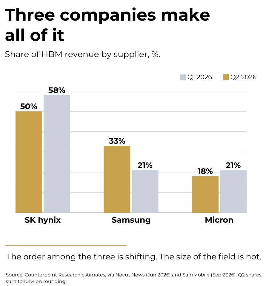
HBM is made at scale by SK hynix, Samsung and Micron. Counterpoint Research estimated that SK hynix held about 58% of HBM revenue in the first quarter of 2026, with Samsung and Micron at about 21% each. By the second quarter, Counterpoint's estimates had moved to roughly 50% for SK hynix, 33% for Samsung and 18% for Micron, as Samsung's newest-generation shipments ramped. The order among the three is changing. The size of the field is not.
The suppliers describe the market as short. Micron chief executive Sanjay Mehrotra told analysts in December 2025 that the company could meet only about half to two-thirds of medium-term demand from several key customers, and repeated it in March 2026. In September he said more than 75% of Micron's 2027 output was already committed. In a July interview with Reuters, SK hynix chief executive Kwak Noh-jung said the company forecasts 2027 to be the worst year in the industry's history from a supply perspective, and expects customer demand to exceed its capacity beyond 2030. These are the companies' own forecasts, and they point the same way.
Why HBM Is Hard to Make
HBM is conventional DRAM rebuilt as a tower. Memory dies are thinned, stacked eight, twelve or sixteen high on a logic base die, and wired together vertically by through-silicon vias (TSVs), thousands of copper channels running through each layer. The finished stack sits beside the processor on a silicon interposer, inside an advanced package, because no circuit board can carry that many connections. The HBM4 standard, published by the industry body JEDEC in April 2025, specifies a 2,048-bit interface and up to about 2 terabytes per second of bandwidth from a single stack. The bandwidth comes from width, not speed.
Each of those features makes the part harder to produce. TSVs consume die area, so an HBM die holds fewer bits per square millimeter than a standard DRAM die, and every bit of HBM uses more wafer than a bit of ordinary memory. Thinned dies are fragile and prone to warping. Yield compounds with height: at 99% yield per bonding step, an eight-high stack comes out at about 92% and a twelve-high stack at about 89%, and one bad layer can scrap the whole stack. In a 2023 test by the bonding-technology firm Adeia, a twelve-die experimental stack yielded 56% overall at 95% per layer. The bonding methods differ by supplier and are still changing, which makes each generation a fresh manufacturing problem.
The consequence is that HBM capacity cannot be added by reassigning existing lines. Converting a DRAM wafer to HBM requires TSV and stacking tools and returns fewer bits per wafer, so every expansion of HBM also draws down the supply of conventional memory.
From Purchase Orders to Contracted Capacity
Memory has long been sold on short contracts and quarterly pricing, which is part of why the industry swung between shortage and glut. That model is giving way to multi-year commitments backed by customer cash.
Micron disclosed 16 Strategic Customer Agreements in June 2026, most of them five-year contracts running through 2030. Its annual report describes them as take-or-pay agreements with binding volume commitments, most with prices held between a floor and a ceiling. Customers post cash deposits, returned if they meet their minimum purchases and forfeitable if they do not; some also post letters of credit. Micron received $12.75 billion in these deposits in fiscal 2026, nearly all scheduled for repayment between 2029 and 2031. SK hynix said in July it had signed long-term agreements with about ten customers, and Seoul Economic Daily reported it plans to require advance deposits. Samsung has not disclosed its terms, but the Korea Economic Daily reported in October that it had committed 75% to 80% of its 2027 memory supply, including HBM, to long-term agreements.
The direction is clear even where the terms are not public. The largest buyers are helping to finance the capacity they intend to consume, and memory is being bought less like a commodity and more like contracted infrastructure.
What the Constraint Changes
For accelerator makers, memory allocation now sets output. A processor without its stacks cannot ship, so yearly system shipments depend on how much HBM each vendor secured, often years earlier. The constraint is already shaping product plans: TrendForce reported in September that Nvidia was weighing HBM with fewer stacked layers for a next-generation accelerator because twelve-high supply may fall short. HBM4's custom logic base dies, designed with individual customers, tie a supplier to specific chip programs and make switching suppliers harder.
For buyers further down the stack, supply committed through 2030 leaves a thin open market: those able to post deposits and sign long commitments secure supply, and later entrants find much of the output already spoken for. Memory procurement becomes a strategic decision rather than a purchasing function.
The constraint also reaches the cost of running models. Serving a large model is often limited by how quickly weights and context move from memory to the processor, so memory bandwidth bears directly on what inference costs. Together with power, which moved to the front of AI infrastructure planning earlier in this cycle, memory is now one of the physical limits on how much compute can be built.
What Remains Unresolved
It is not yet settled whether the new contracts mark a lasting change in how memory is bought, or a long-dated record of the top of a cycle. Memory has a history of overbuilding after shortages. All three suppliers are expanding capacity, and new producers in China are adding DRAM output. The take-or-pay structures were written to hold through a downturn, but none has yet been tested by one. Nor is it settled whether chip architectures that lean less on stacked memory gain ground as HBM stays scarce.
We pays close attention to memory because the pace of the next build cycle may depend less on how fast chips compute than on how fast they can be fed.
Frequently Asked Questions
What is high-bandwidth memory (HBM)? High-bandwidth memory is DRAM built as a vertical stack of thinned memory dies on a logic base die, connected by through-silicon vias and placed beside the processor inside an advanced package. Its bandwidth comes from a very wide interface rather than high signaling speed. The HBM4 standard specifies a 2,048-bit interface and up to about 2 terabytes per second per stack.
Which companies make HBM? HBM is produced at scale by three companies: SK hynix, Samsung and Micron. Counterpoint Research estimated their shares of HBM revenue at about 58%, 21% and 21% in the first quarter of 2026, and about 50%, 33% and 18% in the second quarter.
Why is HBM harder to produce than ordinary memory? Each HBM die gives up area to through-silicon vias, so it holds fewer bits per wafer than standard DRAM. Dies are thinned and stacked up to sixteen high, and yield compounds with every layer, so one defective layer can scrap a stack. Adding capacity requires specialized stacking tools and draws wafers away from conventional memory.
What is the memory wall in AI? The term first described a performance gap: processors computing faster than memory could supply data. In AI it now also describes a supply limit, because the accelerators that run large models depend on a component that three companies make and cannot yet produce fast enough.
Sources
- Edaily, "SK hynix HBM share 58% in Q1 (Counterpoint Research)", June 25, 2026.
- Counterpoint Research, "Global HBM Market Share Q2 2026", September 3, 2026.
- The Motley Fool, "Micron (MU) Q1 2026 Earnings Call Transcript", December 17, 2025.
- The Motley Fool, "Micron (MU) Q2 2026 Earnings Call Transcript", March 18, 2026.
- Stock Analysis, "Micron Technology (MU) Q4 2026 Earnings Call Transcript", September 30, 2026.
- TweakTown, "Micron has signed agreements locking in record-high memory prices with major customers through 2030", June 2026.
- Micron Technology, Form 10-K for fiscal 2026 (SEC filing).
- Gulf Times (Reuters), "SK Hynix CEO sees worst memory shortage in 2027, demand to outstrip supply beyond 2030", July 11, 2026.
- Seoul Economic Daily, "SK hynix Signs Long-Term Deals with 10 Firms, Accelerates Capacity Expansion with Nearly 40 Trillion Won Capex", July 29, 2026.
- DigiTimes, "Samsung reportedly secures long-term contracts covering up to 80% of 2027 memory supply" (citing the Korea Economic Daily), October 12, 2026.
- The Herald Business, "Chipmaker weighs hybrid bonding adoption amid intensifying HBM stacking competition" (citing TrendForce), September 2026.
- Adeia, hybrid bonding stacking and yield results, IMAPS 19th Conference on Device Packaging, March 2023.
- Mobile World Live, "Feature: How the move to custom HBM boosts supply visibility", November 28, 2025.
- HPCwire (JEDEC), "JEDEC Releases HBM4 Standard to Advance AI and HPC Memory", April 16, 2025.
—
Open Doors Partners LLC | Exempt Reporting Adviser
Informational only. Not investment advice and not an offer or solicitation to buy or sell any security. Private investments are speculative and illiquid and may result in loss of the entire investment. Forward looking statements may prove incorrect. Third party data has not been independently verified.
Read full disclosures here.